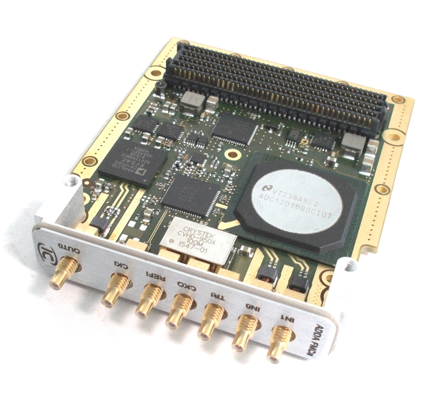
IC-ADDA-FMCa – A/D 12-bit, Dual 1.6 Gsps (One 3.2 Gsps) D/A 14-bit, One 5.7 Gsps
A/D & D/A FMC module
Designed for applications where high data sampling is required, the IC-ADDA-FMCa is a VITA 57.1 FPGA Mezzanine Card (FMC). It offers a flexible connectivity with our FPGA 3U and 6U Front End Processing boards running our Signal Processing Regerence Design (including signal acquisition, Processing DMA Engine, data storage, signal generation,…) thus allowing customers to streamline development of high performance signal acquisition systems by concentrating their efforts on their most critical tasks.
- FMC – VITA57.1 HPC Compliant
- 1 Channel 12-bit, 3,2 Gsps A/D or
- 2 Channels 12-bit, 1,6 Gsps A/D
- 1 Channel 16-bit, 5,7 Gsps D/A
- SSMC Connectors
- Conduction-cooled compliant
- One ADC12d1600 from Texas Instruments™ with 12 bit resolution
- Sampling rate at 1.6 Gsps (3.2 Gsps interleaved)
- 2 channels with SSMC connectors
- Input impedance 50 Ω AC coupled
- Analog input bandwitdth (-3dB) > 5-2200 MHz in Dual 1.6 Gsps channel configuration. Full scale mplitude 800 mV peak-peak
- One AD9129 Analog Devices™ DAC with 14 bit resolution
- D/A sample rate : 2.85 GSPS digital input – 2.85 GSPS output (1x interpolation) – 5.7 GSPS output (2 x interpolations)
- 1 channel with SSMC connectors
- Output impedance 50 Ω AC coupled
- Analog bandwitdth 1.1 GHz in 2 x interpolation mode; 1.4 GHz in baseband mode. Full scale amplitude 1 V peak-peak
- ADC Output : LVDS – Dual data rate – 4 x 12 demuxed data bus. 800 Mbps per LVDS/ 400 MHz clock. Offset binary or two’s complement
- DAC Input: LVDS – LVDS – Dual data rate – 2 x 14 LVDS data. 2.85 GSPS rate/ 1.425 Gbps/ 712.5 MHz clock. Binary or two’s complement


